75rx Engineer Application

If you see this in the last updated topic, no, this is not an engineer application. This is an update to all typos here (September 30 2023).

Before starting to answer everything:

  1. This device wasn’t tested to draw cool animations or programs. I am bad at programming a CPU to run a very complex program in URCLAssembly (this is an edit, I had no idea what was URCL back then).
  2. World download: CPUSRGP (SISD) - CPU-Style Graphics Processor Minecraft Map (hope ORE doesn’t filter it to another dimension.com here)

Minecraft name: 75rx

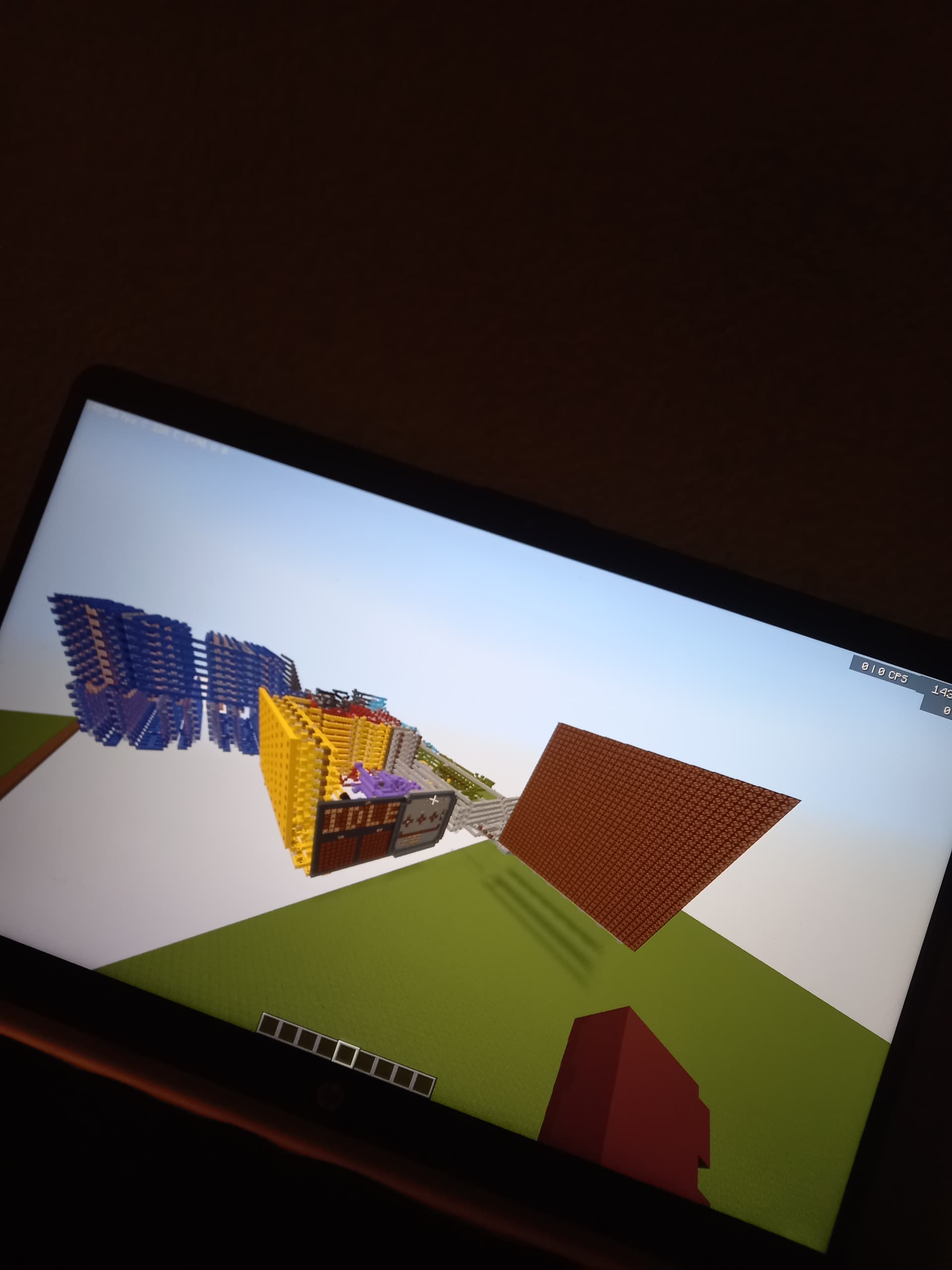
What’s a thing you have made which demonstrates sufficient engineering knowledge?: I’ve invented CPUSRGP (CPU-Style Redstone Graphics Processor). This is something most of players didn’t see.
This is basically SISD, but it is optimized to only render anything. For example, normally you plug X/Y coordinates with the help of I/O, but to create even more useful instructions relative to X/Y coordinates which are easier to do, even giving less headache when programming, I’ve made a special light gray device there. I call it Coordinates Device. Normally it obviously doesn’t exist, but it was decent to easily create awesome and useful instructions in this SISD. Now, you cannot use this as passthrough, unfortunately. But most of players don’t use it anyway.

Time to say specifications.
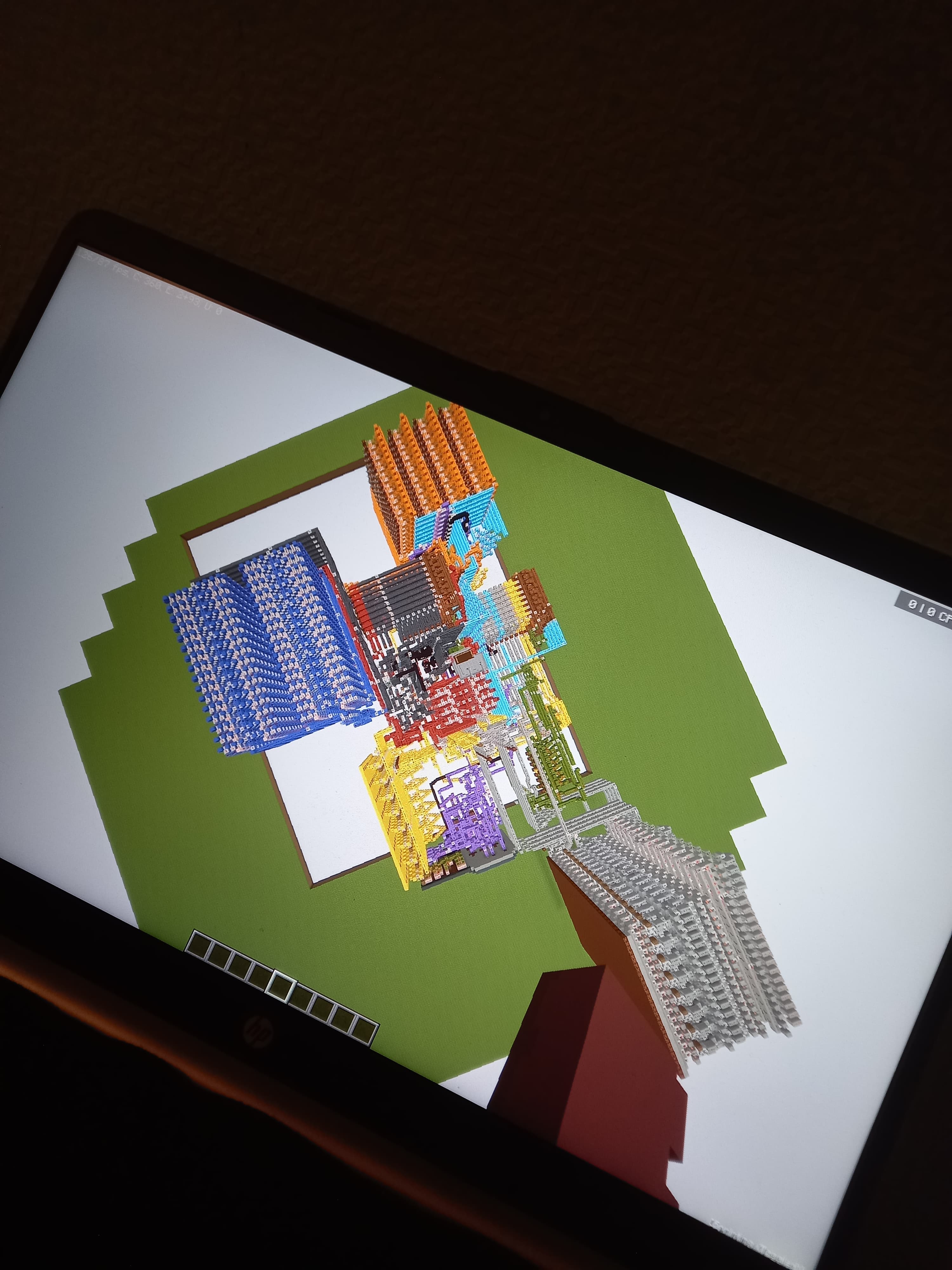
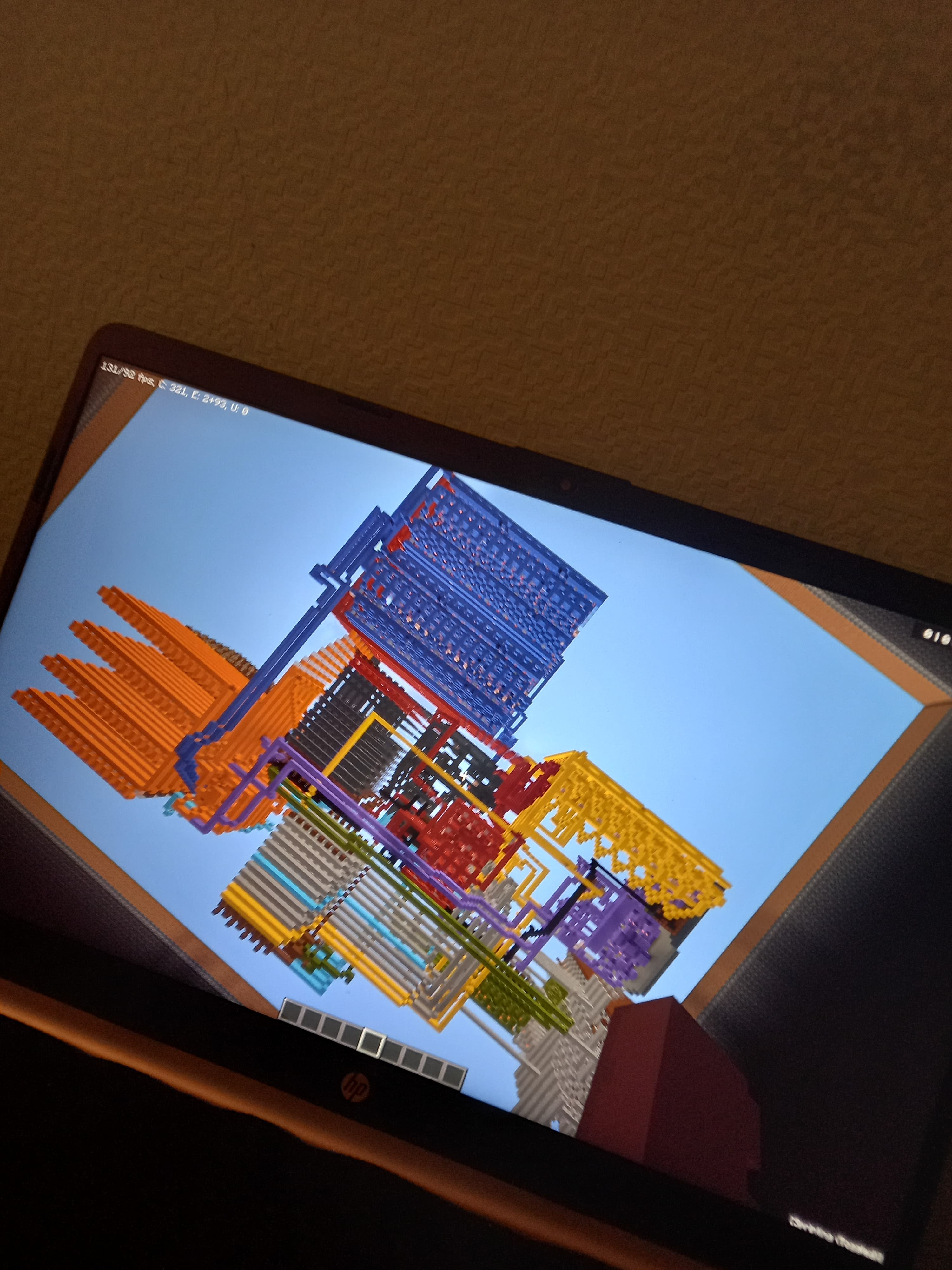
  1. Overall
    -Clock has multiple speeds which you can manage from the UI (User Interface). From 9 ticks which is obviously not recommended (1.11Hz) to 20 ticks for absolute snails (0.5Hz). Clock is purple btw.
    -Program Counter is 6-bit, and default amount of program memory is 64 bytes. Thankfully you can destroy that type of program memory and add iCache with Hex RAM to increase the amount of program memory, or you can move the entire SISD up by a bit and add extra 2 bits to the program counter on the bottom, it will still work. Exactly, this SISD supports 8-bit of PC while it has 6 bits by default. The reason why you have to move is because it’s extremely close to the void - -62 blocks minimum Y height.
    -3 operand RISC architecture with 5-bit opcode, 37 instructions with 8 NOPs, allowing you to add 8 of any instructions you like. This SISD is using MSC instructions (Miscellaneous), which is dark green part. This is to increase the amount of instructions. Obviously the ones that require MSC don’t require any operand.
    -I guess 8-bit instruction length, I am assuming.

  2. RAM (Blue)
    64 bytes worth of data RAM, not shared.
    Addressed with registers
    Serial RAM, probably the same one from the well-known sammyuri’s CHUNGUS2.

  3. ALU (Gray)
    3 tick adder
    Has basic control lines: FC, CIN, !A, !B, LSH, RSH, OR and Output Flood.
    Accumulator and ALU is 1 same device, with the same color coding.

  4. Registers (Red)
    8 bytes of DRR (because of 3 operand)
    Addressed with the help of operand.
    Very small yet fast.

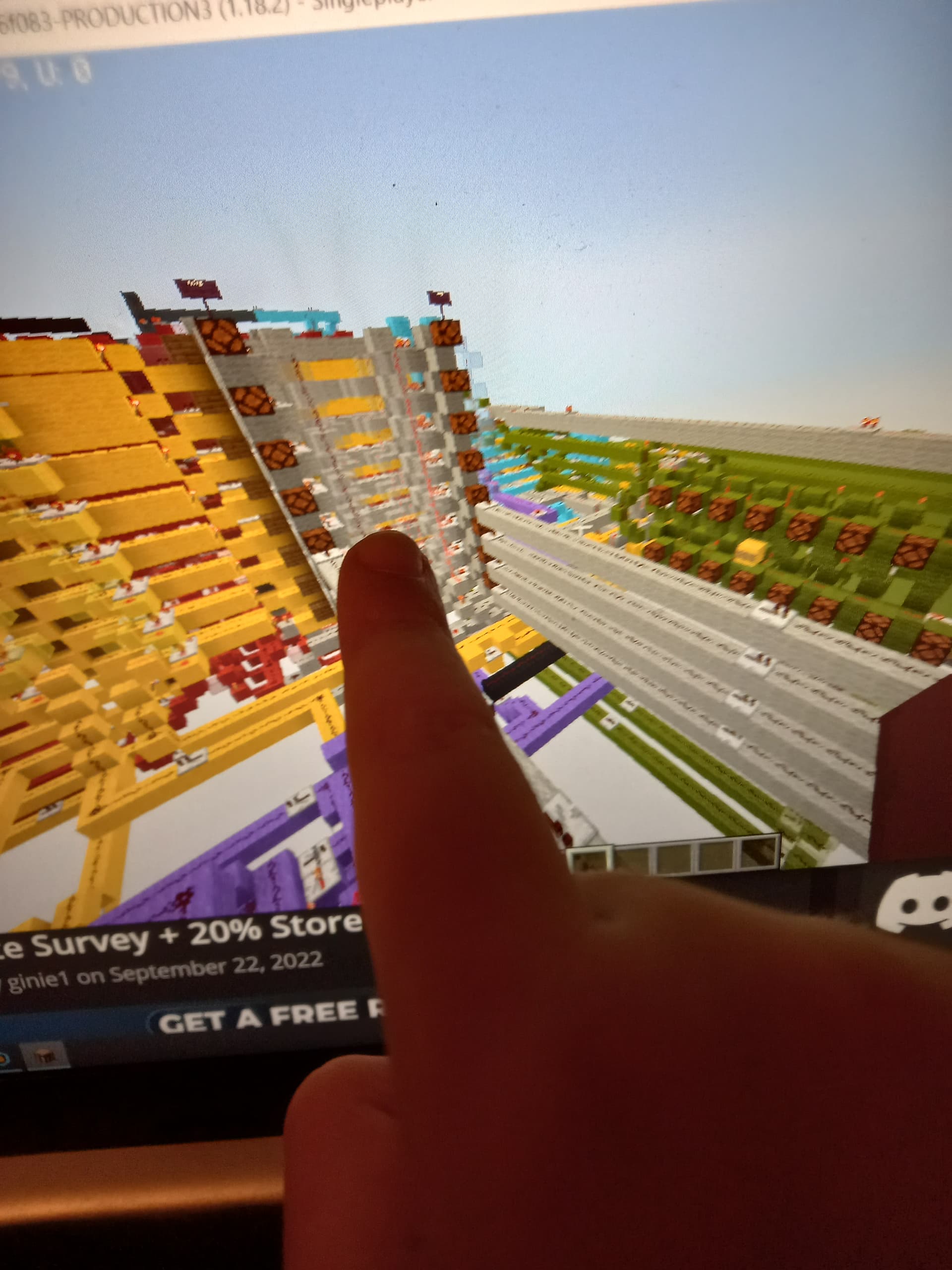
  5. Control Unit (Brown)
    Total amount of CUs: 3. They’re split: one is main, which interacts with ALU, Accumulator and Registers, second one interacts with coordinates and screen, and third one is being called by MSC instruction - so only instructions that can be used with the help of MSC + Operand.
    Has very useful instructions and some my custom ones. With regards “useful”: RPC (Hope it exists, it’s Reset Program Counter), HLT, Pointers, and a lot more. There are 37 instructions and 8 NOPs as explained earlier.

  6. Flags (Black)
    3 Flags: C, !C and 0. This is because I saw these are the most popular flags in 2022 in Minecraft CPUs.
    Flags get ANDed by your operand. I think 100 is 0, 010 is C and 001 is !C. They also get ANDed by the PRD instruction - so there’s triple AND going on. The output of flags will cancel whatever is sending to the CPU, and will also show that one X in the UI.

  7. PMEM / PC (Orange)
    Includes JID/JMP (Pointers) and RPC. As explained earlier.
    6-bit PC and 64 bytes of PMEM. I have already said most of the stuff relative to this.
    Although this SISD isn’t pipelined, immediates obviously are.

  8. Coordinates Device / Display (Light Gray)
    16x16 display. This GPU supports up to 256x256, which is insane.
    Can do: New frame, Reset Display and Draw pixel internally - all with the help of program memory - yes, you can code it that easily - there’s actually the instruction to interact with the screen.
    You can get the coordinates and hook it up into your screen directly here:
    It even tells you which axis is which.

What engineering work went into designing this device?: September 2021 - the month/year of me joining on ORE for the first time. I was slowly becoming better at redstone, but then I saw KilledbytheTV say something like “yeah fibonacci sequence loads like 30% of the CPU”. I teleported to him to see what he made, and oh my gosh, I wish I could run programs myself.

I kept asking for help from players about computer and CPU components. I was learning slowly, but everything was getting better and better.

Oh no! I got banned! I gotta wait for 6 months now.

Okay, finally unbanned.
And then I kept learning even more components and instructions of the CPU - even faster.

Until I made ExecutableMinec- oh. Exactly, that CPU was very buggy. And instruction pipeline(!) was the reason +RAM. Fixing it could take a ton of time.
So, I asked Koyarno about “can I still get an Engineer if I make a good enough CPU-Style GPU that’s not pipelined?”.
He said something similar to yes. Got happy and built this. This CPU is far more stable because it isn’t pipelined. There might be bugs still - I was fixing bugs and modifying world downloads for my EMC2 exactly 10 times(!). This is hilarious, since it still doesn’t work. But this CPU is a lot better.

This is why you should NEVER give up. It’s been exactly a year now and I made this.

What’s even more respectful is I am actually 10 years old (11 tomorrow) and I make stuff like this. Never seen anyone else that’s 10/11 years old make this. I am probably the first one ever.

Image/s and/or video/s of the device:
I’ll upload YT Video soon.
Lol, I cannot take a picture. It says Unable to do this operation because of low memory and then just saves this as a draft. I tried multiple times.
If you still need some images, let me know.

-75rx, September 28 2022.

I haven’t yet reviewed the entirety of the application, but what I have noticed fairly quickly is that I’m not able to gather much about how the build is laid out from just the single image. It might be useful to provide multiple additional images from various angles.

I’ve compiled some thoughts from those of us reviewing the application:


I guess 8-bit instruction length, I am assuming.
I think 100 is 0, 010 is C and 001 is !C

Are you uncertain about the specifications of your own build?


Although this SISD isn’t pipelined, immediates obviously are.

Could you elaborate on this? As far as I’m aware, immediates aren’t something which can be pipelined.


The GPU might be dysfunctional.

This is something you should handle prior to submitting an application with the build.


Your entire section under the question “What engineering work went into designing this device?” doesn’t answer the question itself. It is just various background information on you. What we are interested in is the process from start to finish on your particular build.


-3 operand RISC architecture with 5-bit opcode, 37 instructions with 8 NOPs, allowing you to add 8 of any instructions you like. This SISD is using MSC instructions (Miscellaneous), which is dark green part. This is to increase the amount of instructions. Obviously the ones that require MSC don’t require any operand.
-I guess 8-bit instruction length, I am assuming.

It would also be appreciated to include your ISA somewhere. The stats are neat but there’s no programs or anything to indicate the specifics of the ISA itself.

things

  1. I checked up again, and I confirmed everything. I was correct.

  2. What I mean by that is simple. This SISD doesn’t have any Execute, Decode and Writeback instruction pipeline, except Fetch.

  3. I tested most of instructions, had no time to check them all. But they work as intended.

  4. Okay.
    First, I started building an ALU. That was easy.
    Next, I made flags. That was easy as well.
    Then, accumulator.
    But here’s the fun part. I started making registers, and it started writing every 2 seconds. But it was just 1 dust missing.
    Then, I made RAM. This process was painful, and took me most of the time.
    Next, I made Ports, and the use for them is only to input anything.
    Then, I made the So-Called Coordinates Device.
    After, I was making CU. This took even more than RAM.
    Then, I was debugging CU.
    Then, Program Memory and PC.
    Then, more instructions and CPU debugging.
    Then, screen.
    Then clock…
    Then UI which has a lot of cool functions and had to debug it as well for a bit…
    And finally, even more debugging, until it became this good.

  5. There is already ISA. It comes with the world download. When downloading the world, open the file CPUSRGP_ISA.txt, and it contains ISA.

Is this satisfying now?

ISA Information

Copied from the world download folder for anyone who can’t/won’t download it

CPUSRGP Instruction Set Architecture
CPUSRGP - CPU-Style Redstone Graphics Processor (SISD)

This text document contains everything about instructions, and ISA, AKA Instruction Set Architecture.

00000 | 0 MSC
00001 | 0 RST
00010 | 0 RLD
00011 | 0 ADD
00100 | 0 SUB
00101 | 0 XOR
00110 | 0 PRD
00111 | 0 AND
01000 | 0 IOR
01001 | 0 JID (Pointer)
01010 | 0 MST
01011 | 0 MLD
01100 | 0 LDI
01101 | 0 RPC
01110 | 0 HLT
01111 | 0 Write to Coordinate X
10000 | 0 Write to Coordinate Y
10001 | 0 ADC
10010 | 0 INC
10011 | 0 DEC
10100 | 0 PLD
10101 | 0 ISW
10110 | 0 Update X/Y both at the same time
10111 | 0 Jump to X
11000 | 0 Jump to Y
11001 | 0 Jump to both
11010 | 0 Flood output of ALU
11011 | 0 JMP
11100 | 0 NOP
11101 | 0 NOP
11110 | 0 Reset display
11111 | 0 MSC
OPE001 | OPC00000 Draw pixel internally
OPE010 | OPC00000 Set output of I/O to be X
OPE011 | OPC00000 Set output of I/O to be Y
OPE100 | OPC00000 NOP
OPE101 | OPC00000 NOP
OPE110 | OPC00000 Update X
OPE111 | OPC00000 Set output of I/O to be both X/Y
OPE000 | OPC11111 Update Y
OPE001 | OPC11111 NOP
OPE010 | OPC11111 NOP
OPE011 | OPC11111 NOP
OPE100 | OPC11111 NOP
OPE101 | OPC11111 New frame

Total amount of instructions: 45
Amount of NOPs: 8
Amount of available instructions: 37
Amount of miscelanneous instructions: 13
Amount of miscelanneous NOPs: 6
Amount of miscelanneous available instructions: 7

Opcode: 5-bit
Operands: 3
CPU Architecture: RISC

---------------------------
SISD Halting
---------------------------
The SISD can check if it's halted or not in any way. SISD Halting can be caused from 2 different ways:
1. When the instruction PLD (Port Load) is called and is asking for input to be sent.
2. When the instruction HLT (Halt) is called.
To prevent any bugs, PLD and HLT go the different way of halting. They're just 2 repeater locks switching every time (each for each: one for PLD and one for HLT) and if they're on, they're halted. They literally just depower one single torch (both repeaters).

---------------------------
Instruction cancelling
---------------------------
If the instruction is cancelled, it adds the X to the main menu. If in the UI, X is shown, this means the instruction is cancelled. This is useful for debugging a program, but if your device is a low-end PC and is so bad that literally lags while showing that one X, you can enable Optimization For Low-End PCs in the UI. If you don't know what is it, read another text document.
This CPU has 3 flags: C, !C, 0.
Operand 4 - 0
Operand 2 - C		Warning: Unsure
Operand 1 - !C
These flags get ANDed not only by your operand, but also each by PRD instruction, so it's literally a triple AND. Once the flags output is enabled, SIMD will try to turn off opcode and operand. This is so you cannot only execute any instruction, but also the miscelanneous ones, and even loading immediates.

Yeah. That’s the text document containing ISA.

Generally the expectation is that all information is easily available on the application. This includes images of the build, the instruction set, and other relevant information.

Should I post images about the CPU now?

Yes

You could provide a top-down view and pinpoint each component.

Ultimately, you have to provide programs that it can show and run.

I do not see the added benefit you got here by making x/y dedicated buffers and a screen that can buffer draw calls. You have some more options to save data to these buffers, but that is too little to go on.The least i would expect is some hardware acceleration.
I leave that as an open suggestion.

Here are a bunch of images I made.

Main view:

From the top:

From the bottom:

The middle of the CPU:
“Unable to do this operation because not enough memory” For more images I need to post another reply :frowning:

Those images are really big, for little sharpness. Try to compress them further in the future.
Can’t you just print the screen using f2? (f2 is on your laptop)

I am using a phone bruh

I think it’s made on purpose


Here are X/Y outputs, and they’re getting saved. This isn’t a problem fortunately.

Also the CPU is running a small program, so Y is getting updated.

Note: I was searching around this entire SISD, and found 4 bugs. I recommend redownloading the map if the SISD is buggy.

I would like to hear about what programs this can run, as well as what programs you want to write for it in the future.

Sure. I’ll try my best to code it so it outputs awesome pictures (I can do animations too)

If you could tell us about the programs it can currently run, that would be appreciated.

I did a little modifications to the CPU, and now after that many instructions don’t function as intended. Before showing what it ran, give me some time while I am fixing a little bit of instructions.

If you’re curious: everything gets better and better, I just have to replace these registers with a better design.