Minecraft name:
drzxcv
What’s a thing you have made which demonstrates sufficient engineering knowledge?:
I made a CPU.
Specifications (not exhaustive):
- Accumulator based
- Harvard architecture
- 10 tick clock (1 Hz real-time)
- Three stage latched pipeline (fetch(8 ticks), decode(10 ticks), execute(10 ticks))
- 128 lines of program memory (8-bit bus width for expandability)
- 64 RAM addresses (8-bit bus width for expandability)
- 16 general-purpose registers (some registers can act as pointers for IO/RAM/PC)
- 10 IO ports (8-bit bus width for expandability)
- 8-bit instruction width (5-bit opcode / 3-bit operand, or 4-bit opcode / 4-bit operand)
- Up to 8 explicit branch conditions
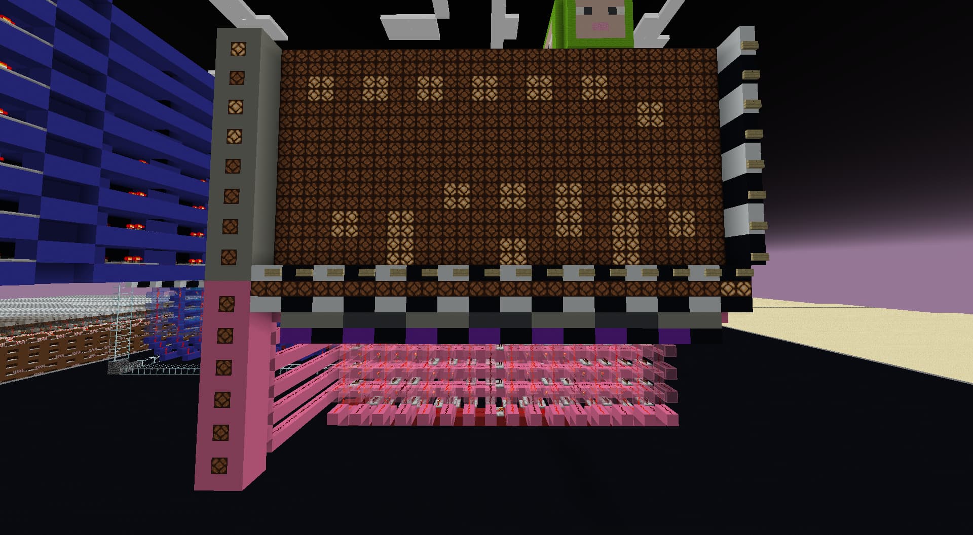
- Dimensions LWH (facing IO ports): 74, 79, 33 (192918 block selection volume)
Features (not exhaustive):
- Compatible with MCHPRS (Minecraft High-Performance Redstone Server)
- Supports absolute and relative jumping (implies subroutines are possible according to my implementation of relative jumping)
- Stack emulation possible (implies call stack and recursion is also possible, assuming validity of the previous bullet point)
- Single-direction static branch prediction (2 clock cycles saved if jump fails)
- 4 easily-customizable branch flags that can be ORed or nOREd together
- Supports multi byte adding, shifting, and rotating through carry
ISA with color legend and programs here.
To elaborate on some of the specifications and features listed above, the bottleneck for the decode stage of the pipeline is located at the general purpose registers where the instruction operand has to go from the latch of the fetch stage to the next latch placed in the data bussing between the registers and the ALU (actually the accumulator, but the ALU and registers are physically sandwiching the latch). The bottleneck for the execute stage also exists near the registers where in the event that a value has been written from the accumulator to the register, if the next instruction requires reading from that same register, it will take 10 ticks from the last latch update for the data to go from the accumulator to the second-to-third stage pipeline latch (same one as mentioned above).
The only delay slots required for this CPU are between instructions that write to the IO or RAM pointer register and instructions that read from IO or RAM to the accumulator. Do note that if the pointer has already been set more than one instruction ago, delay slots are not required. Of course, it is also possible to put an instruction between these two instructions in lieu of a NOP.
For branching flags, they are handled at the accumulator through an 8-bit decoder with four individual “lines”. For example, if the value 0x03 is currently in the accumulator, it is possible to program one of the lines on the decoder to output only if the LSB (0x01) is set (output in this context means that branching will occur if this flag is requested in the instruction). The first 3 decoder lines have already been programmed with LSB, MSB, and zero, however, the last one is still empty for customization. With this approach, it is possible to branch if a specific number or pattern in the accumulator is present rather than using fundamental flags like mentioned above (with less instructions, since this is a hardware implementation). Since there is not a hardware implementation for parity checking, getting information on parity will have to be done programmatically through the ALU’s functions. There is also no hardware implementation for branching using the carry flag, as the carry flag can only be set/reset through ALU-related instructions. Using the carry flag for branching requires using an ALU instruction that moves the carry bit out of the carry flag register (only 1-bit wide) and only then is it possible to branch using MSB or LSB as a proxy for the carry flag.
I filled the entire control unit with instructions, however, some of these instructions are still possible to execute in other ways without having a specific instruction for it. This means that it is possible to change the instruction set a bit to allow for different use cases if a situation that requires it arises.
Relative jumping is handled through constantly reading the program counter’s current address and buffering the output by two clock cycles using latches to synchronize the program line to the current executing instruction, which can then be passed to the accumulator for manipulation.
What engineering work went into designing this device?:
There were three main goals that I had for this project: the clock speed had to be less than or equal to 10 ticks, the CPU’s physical profile had to be a rectangular prism (box), and the instruction width had to be strictly 8 bits wide. Some other aspects that I tried to optimize for were: minimum bussing/control line length, minimum amount of delay slots required for as many instructions as possible, and minimum dataloop delay (an obvious but important one).
After designing and creating my first few CPUs in Minecraft, it became easier to plan ISAs without having to constantly reference parts in-game. This allowed me to start CPU projects by first focusing on designing the instruction set rather than fitting CPU components together and then designing an instruction set around that.
The ISA I had designed for this CPU contained almost everything I currently knew I could implement in-game and it was designed with the main intention of having more flexibility than my previous iterations.
For this CPU, the ISA was first planned out before any construction was done, which allowed me to focus on the design of the CPU rather than the implementation of it. Starting with this approach can have some challenges, as implementation is also a very crucial aspect of a project at this scale. However, as I have already had experience doing this, it would be more beneficial for me to now focus on improving designs at higher levels of abstraction.
Moving on to the hardware section, there are three main parts I want to elaborate on.
Starting with the pipeline, I decided to use the 3-stage FDE (fetch, decode, execute) implementation. This is because I had determined that this was the lowest amount of stages I could have while keeping the clock speed under 10 ticks (which was one of my goals for this CPU). One of the main reasons why I was able to achieve a 10 tick clock with a three stage pipeline was because of the accumulator based architecture mentioned in the previous question. While I was concerned about the restrictions implied by such an implementation, I had thought of some applications where having the accumulator be the main data junction for the entire CPU would be optimal for the instruction set I had planned. (Branch flags being calculated based on the value in the accumulator, for example.)
Improving clock speed past 1 Hz by introducing more pipeline stages for my current design would be impractical for a few reasons. Recall that the tick count for each stage was: 8 tick fetch, 10 tick decode, and 10 tick execute. While it is possible to lower some of these tick counts by using faster components or reducing the distance between them, I had already optimized for these factors in the initial building phase of the CPU. The only other way I could think of to reduce tick count would be to introduce two more stages to my current three stage setup. The reason four stages would be impractical is because there is no easy way to balance the stage bottlenecks by trying to push some of the delay from these 10 tick stages over to an adjacent stage. Only at 5 stages would there be enough freedom to attempt a FDREW (fetch, decode, read, execute, writeback) pipeline, however, as mentioned before, one of the goals was to reduce the amount of delay slots required for as many instructions as possible, and by giving up the benefits of a three stage pipeline for a faster clock speed, this would introduce more mental burden on the programmer to understand the microarchitecture more than they need to (with my current understanding of pipeline bubble remedies).
This next part concerns the registers. For the general purpose registers, notice how there are 16 addressable locations. This would be normal, except for the fact that some opcodes are 5 bits wide (remember that every instruction for this CPU is 8 bits wide). This is where the variable opcode/operand implementation offers an easy solution. Instead of not including eight addresses worth of register space, I combined several two 5-bit opcodes into a single opcode to allow for a 4-bit operand that could support 16 unique addresses (easier to visualize in the ISA Google Sheets). One of the reasons I had chosen to do this is because of the one clock cycle delay slot required when reading from RAM/IO if its pointer was set in the previous instruction. Having more register space allows for certain programs to execute faster without having to utilize RAM as early in the runtime. (Of course, my branching approach benefitted from this opcode design as well due to one additional possible flag condition.)
The implementation for handling immediates is somewhat ad-hoc, as immediates are first loaded into an immediate register by lower and upper nibble and then loaded from the immediate register into the accumulator. As mentioned before, one of the goals for this project is to have one instruction executed per clock cycle, and while it is possible to debate whether or not this approach really saves instructions, one benefit to this approach is that after the initial overhead of loading an immediate, subsequent reads from the immediate register will only take one instruction if the same immediate value is required. (Although in practice, the instructions saved/lost can vary widely.)
This last part concerns the physical form factor of the CPU. The initial stages for arranging the components were fairly straightforward. I took the largest components and placed them around the perimeter of the build (rather, this step defined the perimeter). The component placement was determined through previous knowledge on how different components interact with each other to keep control line and bussing distance to a minimum. After that, I connected the components in decreasing order of bus width (8-bit wide bussing first, then 4-bit for registers, flags, and immediate nibbles, then control and clock lines last).
One final thing I should mention is that I learned a lot from undertaking this project. After completing the build, it became apparent some aspects I could improve in future CPU builds. An example of this would be decreasing required control lines by utilizing the operand more, as there are several instructions that have similar functionality but do not take an operand (like loading values from RAM, IO, PC, or the immediate register by specifying an operand instead of dedicating an entire instruction for them).
Image/s and/or video/s of the device:
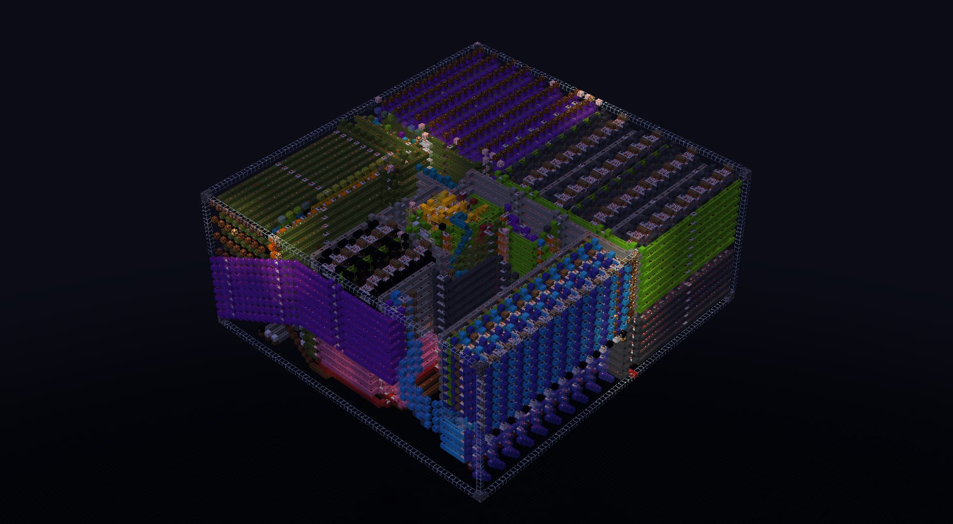
Full view 1
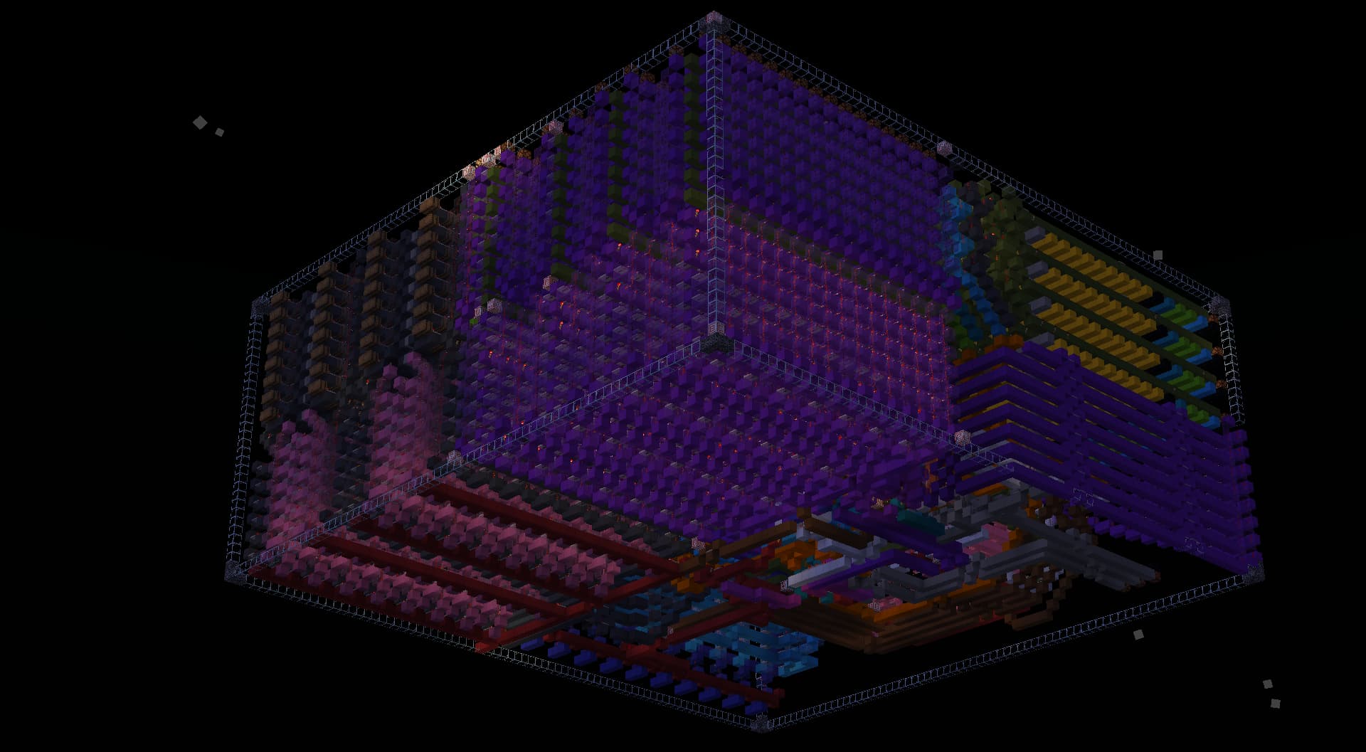
Full view 2

The CPU doing bubble sort on an almost reverse-sorted array

Top down view
At the time of posting this application, progress is currently being made as I move all of the code for the programs I have written for this CPU into the Google Sheets that already contains the ISA and color legend. If someone reading this is disappointed by my current lack of programs, by the time this application gets accepted (if it does), I would have increased my program repertoire to be somewhat comparable to what is seen on other accepted engineer applications, so please be patient as I steadily make progress on this.