Minecraft name: mort96
What’s a thing you have made which demonstrates sufficient engineering knowledge?:
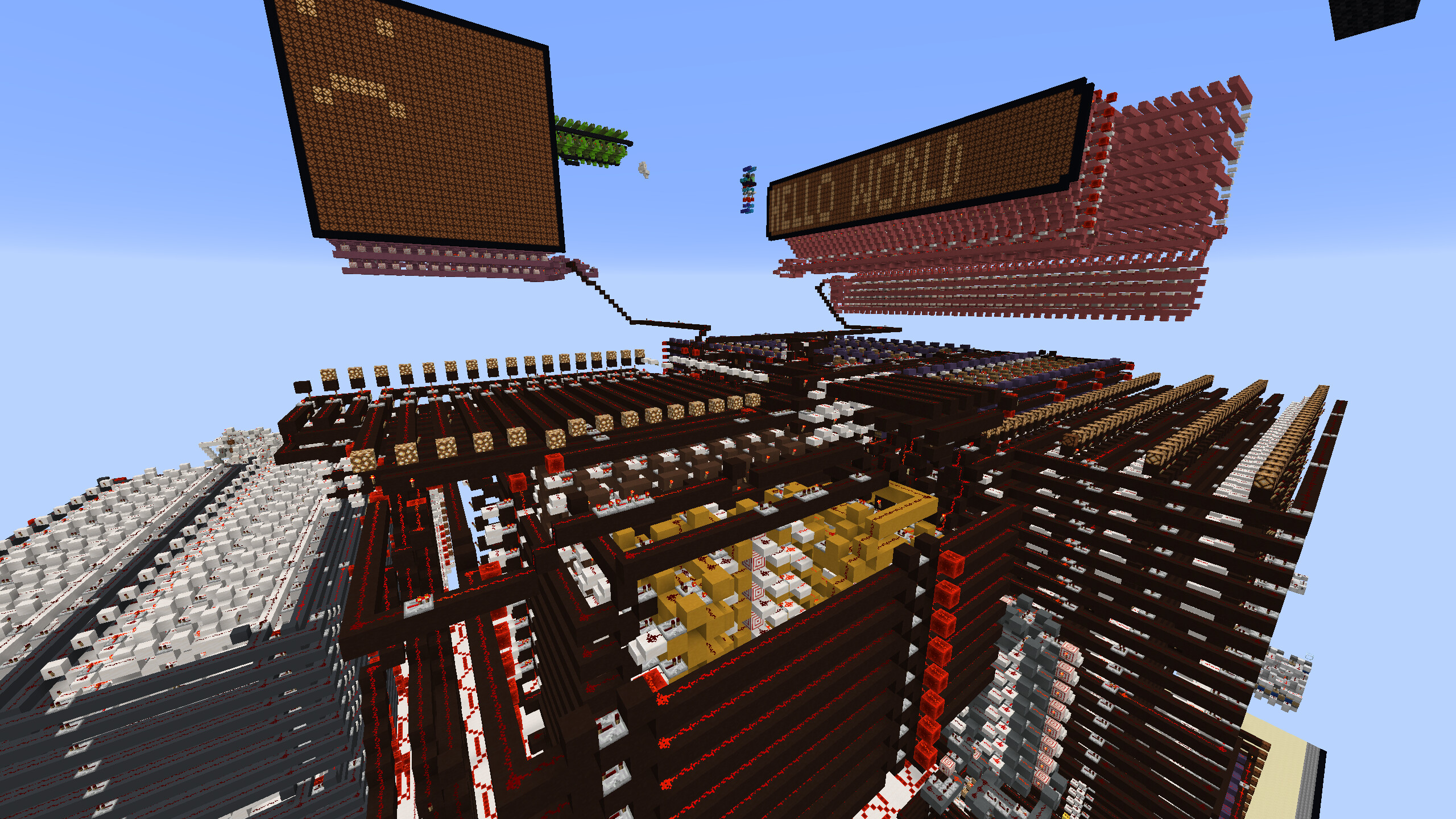
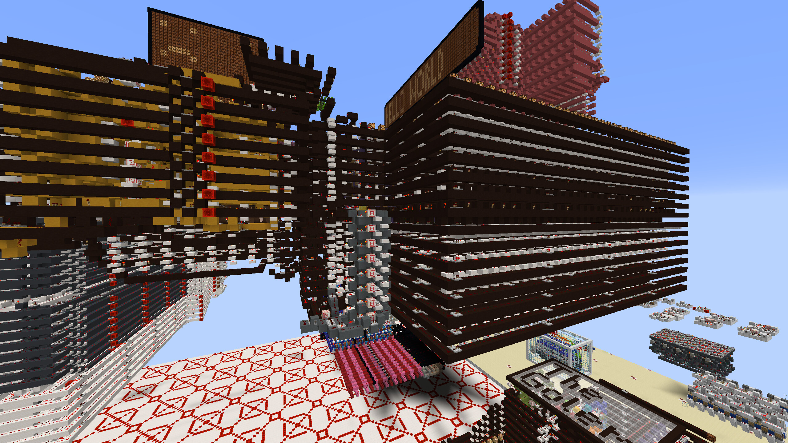
Octornado, my 8-bit Von Neumann style CPU
What engineering work went into designing this device?:
Octornado is a CPU where data and instructions share an address space. It has a 2 (or more, depending on exactly how you count) stage pipeline, and runs on a 25 tick clock. It’s not exactly the fastest CPU ever, but it’s pretty full-featured and has an interesting architecture and instruction set. Before I pipelined it, it needed a 40 tick clock. I could almost certainly push the clock down even more, but I haven’t taken the time to figure out what exactly causes it to miscompute stuff when I increase the clock speed.
The two pipelining steps are 1) instruction fetch/decode and 2) execute/store. You could technically think of RAM reads and writes as being pipelined too, since the RAM doesn’t complete a store in the instruction where the store happens. (There is no fancy forwarding mechanism however; instead, it’s just undefined behavior to load from address the instruction right after storing to it. Due to the design of the ISA, however, this usually isn’t a problem, since you’ll need an instruction between the store and the load in most cases anyways.)
Whenever a branch happens, the CPU actually needs the result of the current computation to know whether and where to jump. So there’s special logic where the CPU figures out if the fetched instruction is a jump instruction, and, if it is, it prevents the normal clock tick from happening, and instead waits a few ticks more until the result of the jump destination computation has reached the program counter.
Pipelining is achieved through timing. So things like control lines aren’t latched, but are instead delayed such that a control line reaches its destination when it should, even if the decoder has gone on to decode the next instruction.
The CPU’s instruction set (and suggested calling convention) is detailed here: Octornado ISA - Google Sheets
Otherwise, the CPU has 128 bytes of actual RAM attached. The rest of the address space is for memory-mapped I/O. A text display is attached at address 254, and a 16x15 pixel display is attached at address 253. The character printer’s protocol is super simple; write an ASCII byte to RAM address 254, and it shows up on the screen. The pixel display is more complicated: each byte stored to RAM address 253 is one pixel coordinate (high nibble for X, low nibble for Y), which sets that pixel on in the back buffer. Sending byte 0xff causes the display to send the image in the back buffer to the front buffer and then clear the back buffer.
I/O is connected using serial I/O ports. I use a repeater-based 2 tick per bit serial system. Currently, the only peripherals I have are output devices, but the system would work just fine for serial input devices as well.
I also wrote an assembler, emulator and schematics generator for the CPU, available in this git repo: GitHub - mortie/octornado-cpu: 8-bit CPU. The workflow for programming for the CPU is something like this: 1) Write the assembly code, 2) assemble it to a binary, 3) run the emulator against that binary to ensure it works as expected (go back to 1 if it doesn’t), 4) run the schematic generator on the binary, 5) upload the schematic and //load it in minecraft, 6), //paste it from a special “schematics paste block”, 7) flip some switches to let the flashing circuit flash the program into RAM. After that, the program is in RAM and the CPU is ready to go.
All parts of the CPU and peripherals were designed by myself, except for the CCA in the ALU. (I know that the engineer rank isn’t about component design though.) Everything uses exclusively “basic” components like repeaters, torches and comparators, with no pistons or observers or hoppers (or minecarts), so the CPU is MCHPRS-compatible.
If I was to redesign this thing, I would make a much more compact RAM design where I design a bunch of RAM blocks rather than scaling up from an individual memory cell design, and I would try to design a variable-length instruction encoding where the vast majority of instructions are 8 bits. I would probably make an accumulator-based design. Spending two whole bytes for every instruction is actually pretty significant. I would also design the dataloop with pipelining in mind from the start, rather than bolting on a limited version like I did here.
Image/s and/or video/s of the device:


Here’s a video which shows the thing running a “Hello World” program: Octornado Minecraft CPU: Hello World - YouTube. The assembly code can be seen on screen, but here’s a link for good measure: octornado-cpu/hello-world.s at main · mortie/octornado-cpu · GitHub - it’s a program which prints a null-terminated string from memory. As such, it demonstrates working with pointers, arithmetic, conditional jumps, and loads/stores from memory. The loop body is 8 instructions, two of which are branches, so it takes a while to run.
