Minecraft name:
oscar91
What’s a thing you have made which demonstrates sufficient engineering knowledge?:
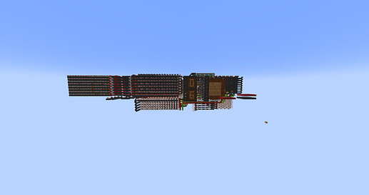
I have built an 8 bit 3 operand rebstome CPU which I have not decided a name for yet. It has got a 4 stage waterfall pipeline (fetch, decode, execute, writeback) running with a rather fast 6 tick clock.
Stats in a list because it’s easy to read =)
-
3 operand
-
6t clock
-
automatic ALU forwarders
-
4 stage waterfall pipeline
-
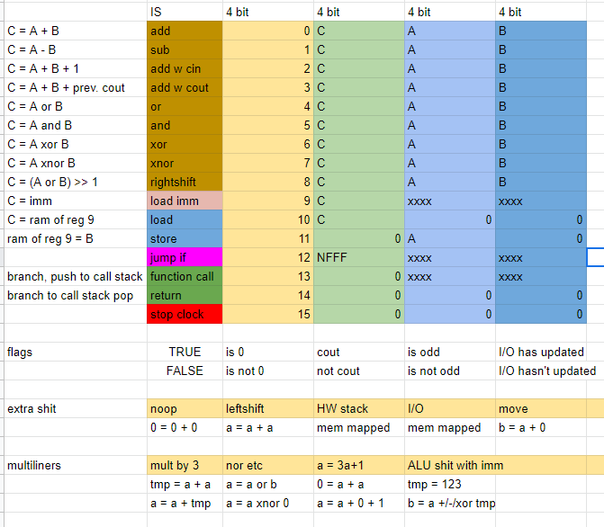
4 bit opcode, see ISA for details
-
8.5 simulated dual read ALU-register, 8 general purpose, and a 9th doubling up as the pointer
-
0-register, as well as temporary imaginary registers, more on that later
-
128B instruction cache (64 instructions at 16b per instruction)
-
64B RAM (accessed by pointer)
-
4 memory mapped IO ports
-
1 (one) memory mapped hardware stack for optimized stack usage
-
call stack for recursion
-
up to 8 flags with 16 branch conditions, currently has 4 flags with 8 conditions installed (carry out, odd, zero, input) with the ability to test for all flags inverted
This CPU is engineered using everything i learned from building my first pipelined CPU. My goal was to create a more powerful and capable machine suited for more advanced programs, which I very much succeded with. Originally i was going only improve my previous one, but I became more ambiguous and created a completely new architecture from scratch. The only similarity is the ISA, which is made out of 4x4 bit “chunks”; opcode, operand1, operand2, operand3. For non 3-op instructions, the operands can represent something else, like branch conditions, immidiate values, and branch destinations. Having call-return instructions with a call stack is the biggest improvement in the ISA.
Further improvements in usability and programmer friendliness was made by using a repeater lock i-cache instead of torch ROM. It allows me to store multiple programs in the world and easily load them. This could be expanded to use automatic page swaps but I have not implemented that yet. My 16-bit instructions are stored in 2 seperate 8-bit i-caches, similar to CHUNGUS which allows for shorter bussing and a nicer layout in my case.
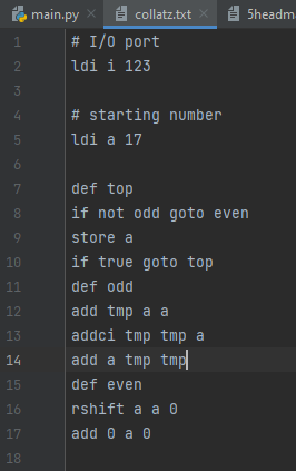
A custom assembler was made with python to convert assembly code into a schematic file that you can paste in the world. It is not currently very feature rich, but it does support lables for branching, and comments as well as blank lines will be ignored. I used a tool created by Sloimay to generate the .schem file.
The ALU-register loop is 12 ticks, but thanks to the automatic 6 tick forwarders there is no data hazard when using the ALU. If the control unit notices that one of the regesters being read from is the same as the one being saved to in the previous instruction it will automatically forward at 0 cost. This works for both the A and B input, and it will ignore the operands if the instruction should not forward, like an immidiate load or branch instruction. The forwarders host one of my favourite features about the CPU which I call “temporary registers”. A temporary register is an adressable register that does not exist in hardware. Registers are adressed with 4 bits but there are only 9 registers in hardware (1-9). If you try to save to r0 or r10-r15 it won’t save anywhere (but its used to update flags without overwriting). If you try to read from them they will give 0, unless you previously saved to it, in which case it will forward the previous ALU result. An exception is made to r0, which can’t be forwarded giving the programmer confidence that it will always give you a 0. The forwarding of r10-r15 is actually useful for multi-line ALU operations without overwriting any register. An example would be to multiply a register by 3 without using any other register. You can also use it to add with immidiates. The psuedo code would look like this:
# a = 3*a
tmp = a + a
a = a + tmp

# a += 13
ldi tmp 13
a = a + tmp
The RAM and other memory mapped devices are adressed with with r9, and has a 7-bit adress space. Currently the RAM uses adress 0-63, IO uses 123-126, and the stack uses 127. The memory mapped space could be expanded to 8 bits but as I currently only use 69 adresses I decided to let it be 7 bits. Reading from RAM, IO, and stack has no delay slot so the value could be used in the forwarders in the next clock cycle. The catch is that the pointer needs to be updated 3 cycles before reading. When writing you only need to update the pointer 2 cycles before as writing to RAM is later in the pipeline than reading. To get somewhat fast sequential read and write you can pipeline the operations like updating the pointer 3 times then reading 3 times.
The most advanced program I wrote on my previous CPU was shift-add multiplication (but the one that impressed most people could open and close a piston door). This new CPU is much more capable and examples of programs ive written are:
-
Fib
-
Collatz (it gets better)
-
fizz-buzz
-
Recursive stuff using the call stack
-
N-element insertion sort
The maximum amount of elements I have sorted is 64, which is my entire RAM. It took 15 seconds on MCHPRS without optimization.
But can it run doom?
-Yes!
*I not actual doom
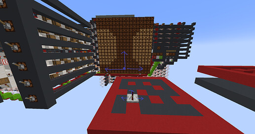
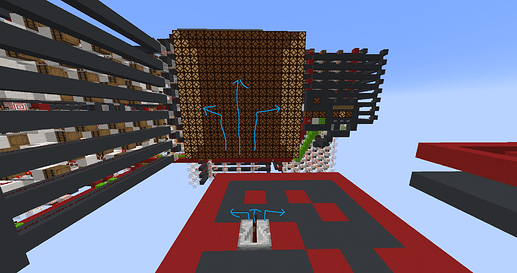
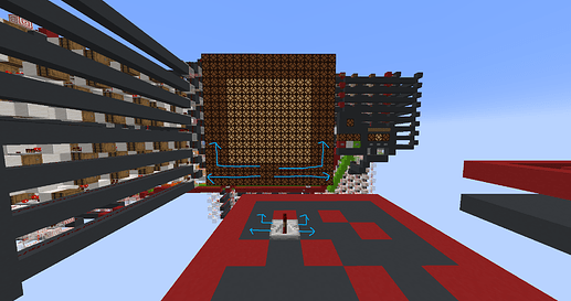
My favourite program I have written so far is “doom”, which is a psuedo 3d maze explorer. You, as the player, can walk around freely using the I/O for controls, and the CPU will detect the 5 closest walls relative to your position and rotation, and display them on a psuedo 3d display with 9 segments. You can chose to rotate left, rotate right, or walk forwards. You are not able to walk through walls.
What engineering work went into designing this device?:
As I previously mentioned I put effort into designing an ISA that allowed for more complex programs. Features like call-return, rightshift, more flags, and better control over flags were implemented. The ISA is designed to use four 4-bit chunks which allows for very easy decoding as well as easy programming.
The custom assembler completely throws away all effort I made to have easily readable machine code, as I never need to touch machine code again, but overall it is a great feature which has helped me a lot. The syntax I created for the assembly language is based on the machine code in the sense that you type a keyword (roughly translates to opcode) as well as any other information needed, like registers, numbers, flags etc. Digging deep into the assembler might not be relevant here but I will happily answer any questions about it.
A 1.66Hz clock is decently fast in the redstone world, and it comes with a few design challenges. The most notable is the requirement of pipelining. I had previously built a CPU with a 6t pipelined clock, so I knew what problems might occur. I went with a waterfall pipeline because I did not feel like I would need latches. I was confident in my tick-counting skills and the CPU did turn out fine. The biggest timing challenge I faced was to get my ALU-forwarder-inverters to work. The signal can travel through a repeater or a torch, where one of them will be blocked, creating a 1 tick togglable inverter that also boosts the signal. The design was inspired by MPU7. For this to work you need everything in the dataloop to be pulsed, or you might accedentally lock a repeater with a value. Registers, RAM-I/O reads, and alu operations all need to work on 2t pulses. This did not cause me too many problems as I had carefully counted all ticks.
A second challenge with pipelining is branching. My conditional branching require 4 delay slots which might seem like a lot of wasted program space, but decided to let the CPU execute all of them because I was able to cram in useful instructions in the delay slots in most of my programs. An alternative would be to temporarily stop the clock so only 2 delay slots would be executed. If I didn’t want to waste any program space I would have needed to “force a noop” on the first two delay slots as the clock cant stop in time for them. I am yet to run out of program space because of the delay slots, and they don’t cause performance issues, so I have decided to keep them. Function calls, returns, and halting has 2 delay slots.
I have designed every component myself from scratch, which might be notable to name. The reason being that I feel pride knowing that I understand everything about every component. It might be worth mentioning that the i-chache is the “usual one” found in many CPUs, as its simply a great design that I was unable to improve.
Image/s and/or video/s of the device:
ISA
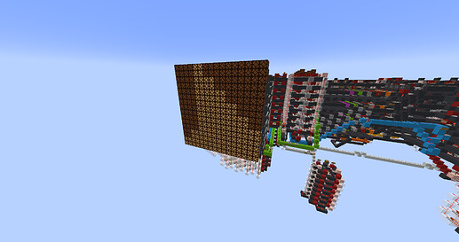
8 element sort shown on a display
doom: repeater is the player
I painted these blue arrows to make it easier to understand the perspective, as its hard to show on a 2-color display.
I hope it is clear by now… maybe I’m bad at making displays?
Sign fever
Assembly code example
