Minecraft name: Q2CK
What’s a thing you have made which demonstrates sufficient engineering knowledge?:
I built the AnPU 1 - a horizontal redstone CPU that so far managed to run programs such as: n-element bubblesort (up to 32), collatz conjecture, 32-bit fibonacci sequence, 16-bit multiplication, and my favorite - a 1-player pong game that KilledbytheTV was kind enough to write for me when I ran out of steam ![]() That pong program is sort of a proof of accomplishing the main goal of AnPU 1 - the ease of programming, without worrying about unexpected hazards and dependancies. More details on that further below.
That pong program is sort of a proof of accomplishing the main goal of AnPU 1 - the ease of programming, without worrying about unexpected hazards and dependancies. More details on that further below.
Video presentation (with great thanks to mattbatwings for a shoutout on his channel): AnPU 1 | A 1.43 Hz Horizontal Redstone CPU - YouTube
- 7 tick clock
- 4 stage waterfall pipeline
- No unhandled hazards, very easy to program
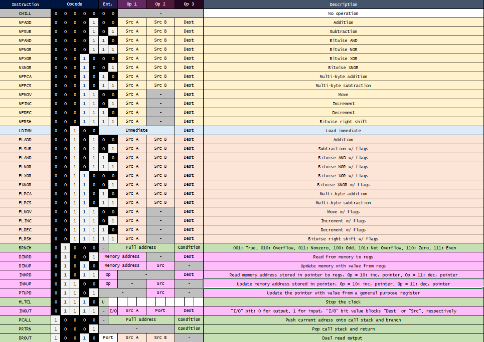
- 12 ALU operations
- Automatic ALU forwarding on both inputs
- 8 dual read registers
- 256 B of main memory
- 32 B of data scratchpad / cache
- 64 B (32x16 bits) of instruction cache
- Automatic instruction cache page swaps
- 7 branch / call / return conditions
- 8 I/O port pairs
- 16 line hardware call stack
- Pointer register with instant increment/decrement option
- Fast 8+ bit addition / subtraction / right shift
What engineering work went into designing this device?:
AnPU 1 is mostly made of components designed by me from scratch. It’s worth pointing out that the reason for it wasn’t any kind of “desire to be original”, which often comes at a cost in efficiency. It was motivated by the fact that after looking through the internet I just wasn’t able to find parts with the specifications that I needed. That includes:
- 5 tick ICA ALU, containing a 4 tick synced Instant Carry Adder. There are a few well-known designs of ICA, but I found them difficult to use due to their piston-based output XOR gates which have a tendency to generate annoying 0-tick pulses. Another reason was their unoptimal shape for what would later become probably the first horizontal simulated dualread dataloop of this kind. Thanks to its automatic forwarding, this type of dataloop is actually capable of operating at up to 2 Hz, which I will happily use in AnPU 2.
- 2x2 horizontal memory bits. The memory is perhaps the least self-designed part of this CPU, because it’s very much based on what n00b_asaurus showed on youtube several years prior. However, with the help of Acerixx and FEARLESS_Z, we were able to make the old memory design one block less tall, which later turned out to be the only reason my instruction cache design was able to work at the desired speed
 I ended up liking this memory so much that I used it as my SDR registers, the data cache AND the instruction cache, awesome
 - Sophisticated CU (at least compared to most horiz CPUs), which prevents any kinds of hazards by introducing instruction cancels and by enabling ALU forwarding whenever needed. All data in the CPU has to travel through the ALU first, which allows the forwarding to work regardless of whether the data arrived from the registers, the cache, the IO ports or the immediate bus. You can also switch the CPU to what I call LIKWID mode (Lmao, I Know What I’m Doing), where the cancelling is disabled and the user can exploit delay slots, at the expense of increased programming difficulty. Forwarding is available either way as it doesn’t introduce any delays.
- Other, more minor components: horizontal call stack, which is loosely based on Kazik24’s design, just made far more compact than originally, horizontal IO ports with 2x2 bits and budswitch memory, ICA based program counter with the ability to branch and retreat by 1 (this is needed for proper execution of the 2 instructions that get cancelled when required), incrementable and decrementable pointer register, and finally a 2-tick cycle, 16-bit sequential BCD decoder.
The basic aim for this CPU was for it to be Horizontal™. Horizontal CPUs bring up some good memories of the early redstone tech, and overall have a great aesthetic appeal. And as it turns out, they don’t necessarily have to be worse than vertical designs. For ORE members, this might automatically sound like an unnecessary step backwards, but it really isn’t.
The first step was to create an adder, and ultimately an ALU, that would be comfortable to build around, while matching or even beating the speeds of vertical ALUs. I chose ICA because it provides the lovely delayless carry without the bulkiness of CLE adders, the size and confusing wiring of CLA, and the near-impossible or at least unpractical feat of engineering that a horizontal CCA is.
I started off by grabbing the commonly known input XNOR that bennyscube showed in his video on why ICA adders are not a good choice. Then I threw away the entire second half of the adder and replaced it with the very same 2 tick XNORs, which was all that it took to eliminate the 0-tick pulses that ICA users always complained about. Well… almost everything, because for the adder to work in sync, without sending out any kind of weird noise, I also had to run the entire CPU on pulsed signals – 3 ticks of data and 4 ticks of cooldown in every part of AnPU. Since it’s a waterfall pipeline, pulsed instruction cache reads were all that it took.
Then, the adder was completely reshaped into a T-like configuration, with inputs coming from both sides at the bottom of the adder, and the output coming out both ways at the top. This allowed me to easily use the previously mentioned piston memory and the ALU forwarding on both inputs. Like that, a 5 tick simulated dualread ready ALU was made.
Why a waterfall pipeline? Because as much as I like the idea of latched, there’s just no convenient way of making 1-tick horizontal D latches like in vertical. An added difficulty here is that all signals in AnPU have to meet at exactly the same places and times, otherwise the sensitive ICA adder would no longer work sustainably. Pulsed signals actually made it easier to visually determine desynced wires and fix them.
After having built 6 NISC-like CPUs I knew it was time for a more reasonable instruction set, which would be understandable for outsiders and which would allow me to write programs quickly, unlike with my previous creations which were a nightmare in that aspect. Programming is also made much easier by the fact that, as I already mentioned, the user doesn’t have to worry about any kind of dependancies between instructions. Data hazards are instantly handled by the forwarding. Hazards related to flags, branching and pointer updates are handled by just “waiting it out”. That means cancelling 2 following instructions, and then returning to them. A good thing is that branches, calls and returns will only cancel when their condition is true. If that’s not the case and the branch/call/return doesn’t happen, it won’t cancel and will proceed without any extra delay. Cancelling can also be easily disabled, which would allow the user to abuse delay slots and squeeze an extra bit of speed out of the AnPU 1 for the cost of complexity of programming.
To input the programs easily, I added an 8-line “flasher” circuit that loads a fragment of your program into the main memory.
Speaking of the main memory, it is 256 Bytes of Chungus 2-inspired repeater-lock memory, but horizontal of course. The instruction cache is 64 Bytes in capacity, so the main memory is divided into 4 pages. Each quarter of the main memory is hard-wired to a quarter of the instruction cache, which together with its 2 ticks/bit, allows for 5 second cache reloads. AnPU 1 will reload the instruction cache whenever the 2 oldest bits of the 7 bit branch/call/return address don’t match with the stored 2 bits that identify a currently loaded page. The cache doesn’t reload after the PC reaches 31 – this is doable, but I put it aside for now, because I found it really complicated to construct without ruining the fun properties of branching in AnPU. The memory consumed a very big part of the time I spent on this CPU, because I made a few mistakes with timings that were hard to find and correct.
As a matter of fact, so many mistakes were made in the making of this CPU that the one you see in this post is the 4th iteration. Initially, I was aiming for a 6 tick clock, but ultimately decided to lower it down to 7 ticks for CU reasons. This is why the forwarding mux is made of locked repeaters – it looks like a latch, but it really is timed in such a way that it works as a signal-extending mux. Comparators don’t extend the signal, so if I were to use a comparator I’d have to add an extra repeater, creating a 7 tick loop. Now that I went for 7 ticks, this would work just fine, but because I already got it working on the 6 tick version I decided not to touch it and simply add the extra tick without swapping the locked repeaters for comparators.
Image/s and/or video/s of the device: